registered   |   log in
  中文

北科产品中心 products center

MXenes-Max 2D transition metal carbonitride
MBene two-MAB-dimensional transition metal borides
MOFs metal organic framework compound
COFs covalent organic compound
Bioluminescent dyes
Aerogels
CVD TMDC 2D thin film / heterojunction
Perovskite material
Copper-doped modified lead apatite (LK 99 crystal powder)
2D material fiber/film
Two-dimensional material micro-nano processing - in situ testing
Basic magnetic beads, immunomagnetic beads, protein purification magnetic beads, nucleic acid extraction magnetic beads
Nucleic acid extraction kit
High-entropy materials
Biological nanomaterials
Nanocellulose
AIE luminescent material
Silane Bismuthene Borene Tellurene Phosphorene Graphyne
Binary CVD TMDC crystal/powder/dispersion
Ternary CVD TMDC crystal/powder/dispersion
Graphene and carbon nanomaterials
High-performance battery materials
Carbon nanotube/fullerene series
Nano/micron powder material and AAO template
Nanowires
Molecular sieve
Ionic liquid
QDS
Nanomaterial customization / material simulation calculation
Metal nanomaterials
Hydrogel Series and Consumables
Solid-state lithium battery
Product Solutions
Industrial-grade nanomaterials
Special materials for sodium storage
Thermoelectric materials
Organic materials
Atomic catalyst
Mesoporous materials
Heavy launch-new products are online!
Two-dimensional layered double hydroxide
catalyst
Nanosphere
Material testing and consumables
Inorganic Nanomaterials
equipment
MXenes 2D transition metal carbonitride
MBene two-dimensional transition metal borides
beike new material
position: home > Product > CVD TMDC 2D thin film / heterojunction

Custom stripped heterojunction devices


ID:BK2020100202
CAS:
Detailed

1. Technical guarantee: a team of top domestic technical engineers. (More than 5 years of related work)

2. Preparation conditions: complete advanced experimental equipment, complete two-dimensional materials (except special materials), customers only need to provide device structure diagrams.

3. Manufacturing cycle: The material peeling characterization is transferred to the device to complete the entire process. The delivery period will be slightly different according to the difficulty of the two-dimensional material peeling. Normal delivery time is about 1~2 weeks

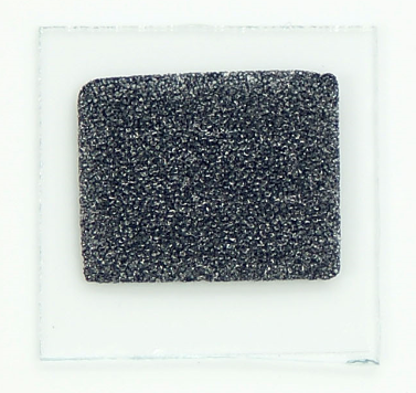
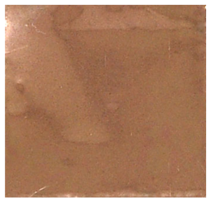
4. Material surface cleanliness: The material surface is atomically clean.

5. Different materials, different materials and different layers of heterojunctions can be customized

Warm tip: the products supplied by Beijing Beike Xincai Technology Co., Ltd. are only used for scientific research, not for human body

Message
Full name: *
Whatsapp/Wechat: *
E-mail: *
Contents:
 
Twitter:2D materials Frontier
QQ Exchange Group:1092348845


Reminder: Beijing Beike New Material Technology Co., Ltd. supplies products only for scientific research, not for humans
All rights reserved © 2019 beijing beike new material Technology Co., Ltd 京ICP备16054715-2号
advisory
phone
Email:mxenes@163.com
Tel:+86-17715390137
scan

scan
WeChat