|
Substrate
|
specification
|
price
|
Square resistance (Ω/□)
|
|
SiO2/Si-based double-layer graphene
|
1cm*1cm
|
Inquiry
|
300-500
|
|
SiO2/Si-based double-layer graphene
|
2cm*2cm
|
Inquiry
|
300-500
|
|
SiO2/Si-based double-layer graphene
|
5cm*5cm
|
Inquiry
|
300-500
|
|
SiO2/Si-based double-layer graphene
|
Other size
|
Inquiry
|
300-500
|
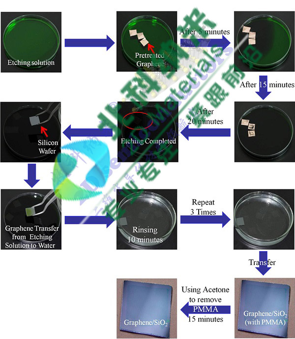
Copper-based graphene transfer technical parameters
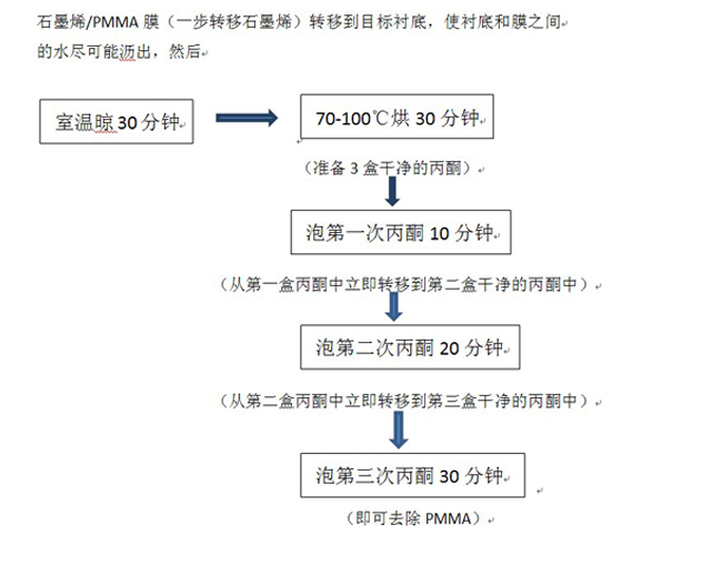
Schematic diagram of copper-based graphene transfer process:
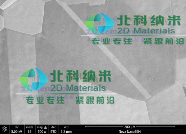
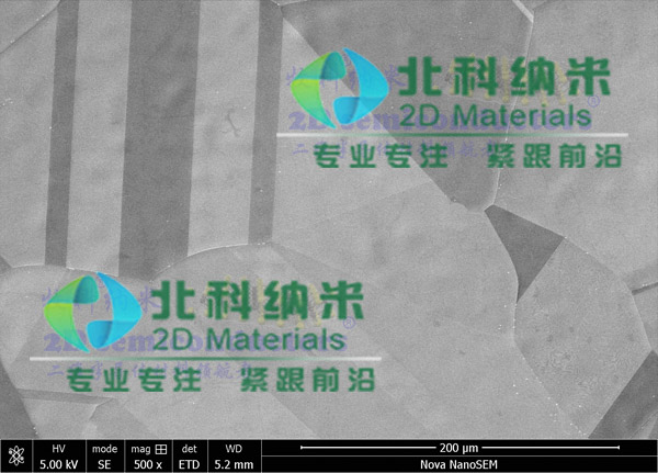
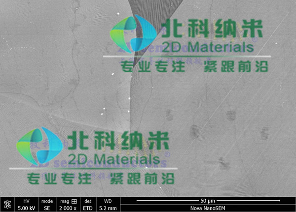
Graphene characterization data:
SEM:
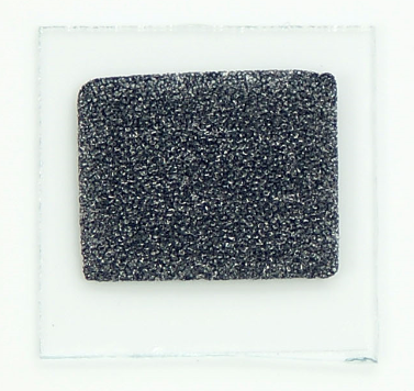
SIO2/SI-based graphene photo:


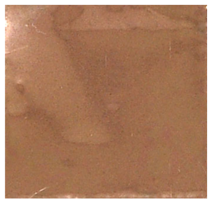
Optical microscope photo:

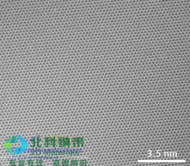
High resolution transmission electron microscope photo:
High electron mobility of graphene film tested by photolithography (EBL engraved electrode will be higher):

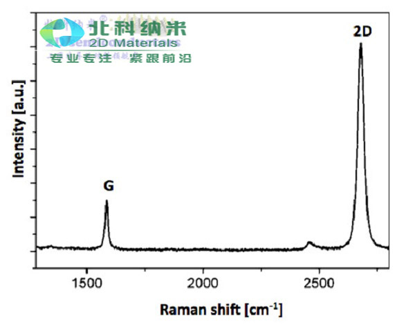
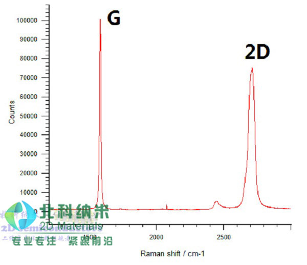
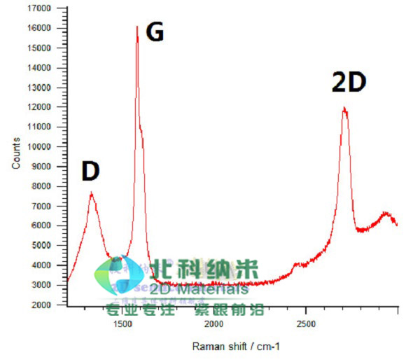
Raman spectroscopy data:
Single layer graphene Raman spectroscopy
Double layer graphene Raman spectroscopy
Three-layer graphene Raman spectroscopy

|
Warm tip: the products supplied by Beijing Beike Xincai Technology Co., Ltd. are only used for scientific research, not for human body |
| Item ID |
CAS |
ID |
Pack |
Parameter |
Stock |
Make up |
Price |
| BK101664-01 |
7440-44-0 |
BKMK237 |
|
1cm*1cm |
100 |
|
$0 |
| BK101665-01 |
7440-44-0 |
BKMK237 |
|
2cm*2cm |
100 |
|
$0 |
| BK101666-01 |
7440-44-0 |
BKMK237 |
|
5cm*5cm |
100 |
|
$0 |