 Our company is currently able to manufacture high quality monolayer molybdenum disulfide films.
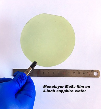
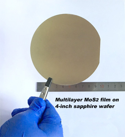
The largest 4 inch discs are currently available, and larger sizes (8, 12 inches) are coming soon.
Basic properties:
Undoped molybdenum disulfide is a layered N-type semiconductor ,which belongs to a transition metal dichalcogenide with a bulk band gap of 1.23 eV (indirect band gap) and a single layer MoS2 band gap of ~1.85 eV (direct band gap).
Production method:
Chemical Vapor Deposition (CVD)
Product introduction:
Molybdenum disulfide films have sevaral kinds:
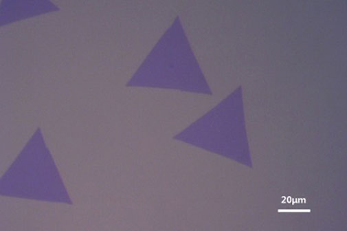
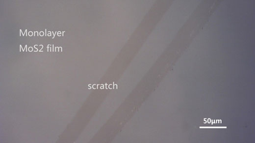
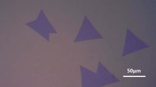
1) A single-layer discretely distributed triangular single crystal grain whose triangular side length is generally several tens to one hundred micrometers.
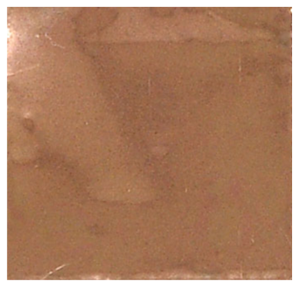
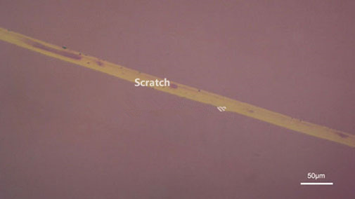
2) A single-layer continuous film that continues to grow in Dalian by triangular grains.
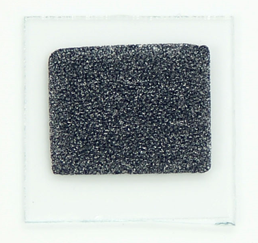
3) Multilayer MoS2 continuous film.
4) Substrate: MoS2 has many optional substrates, among which the most commonly used silicon substrate, the oxide silicon substrate and the sapphire substrate are direct deposition products. Other substrates such as PET, PI, ITO, FTO, glass, metal substrates, etc. are transferred to the substrate desired by the customer after growth on sapphire.
The oxide layer has a thickness of 300 nm or other thickness.
Application fields:
Optoelectronic devices, microelectronic devices, biosensing, chemical sensing and other fields.
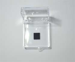
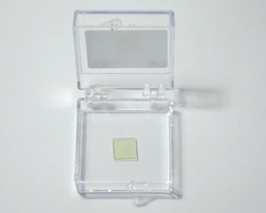
Packaging and specifications:
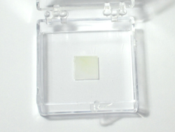
10 * 10mm, 15 * 15mm, 20 * 20mm, 2" disc, 4" disc or custom size specified by the customer.
Purification vacuum packaging, 1 piece / box, 5 pieces / box. 10 pieces / box.
Typical customers include:
Massachusetts Institute of Technology, California Institute of Technology, Stanford University;
Oxford University, Manchester University;
Seoul National University, Korea Institute of Science and Technology (KAIST), Sungkyunkwan University;Tokyo Institute of Technology, Murata Manufacturing Co., Ltd.,Tsinghua University, Peking University, Institute of Semiconductors, Chinese Academy of Sciences,And other world-class research institutions.
Single-layer MoS2 isolated single-layer MoS2 continuous film

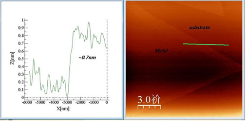
AFM data of MoS2
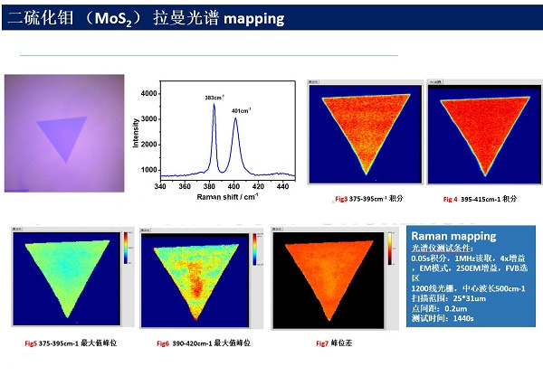
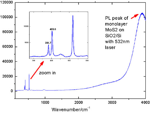
Raman shift of MoS2
MoS2 film on SiO2/Si substrate
MoS2 film on quartz substrate
MoS2 film on sapphire substrate
Single layer MoS2 Multi-layer MoS2
Reference:
1)Gao, Min-Rui, Jin-Xia Liang, Ya-Rong Zheng, Yun-Fei Xu, Jun Jiang, Qiang Gao, Jun Li, and Shu-Hong Yu. "An efficient molybdenum disulfide/cobalt diselenide hybrid catalyst for electrochemical hydrogen generation." Nature communications 6 (2015): 5982.
https://www.nature.com/articles/ncomms6982
2) Radisavljevic, Branimir, Aleksandra Radenovic, Jacopo Brivio, I. V. Giacometti, and A. Kis. "Single-layer MoS 2 transistors." Nature nanotechnology 6, no. 3 (2011): 147.
https://www.nature.com/articles/nnano.2010.279
3) Wang, Qing Hua, Kourosh Kalantar-Zadeh, Andras Kis, Jonathan N. Coleman, and Michael S. Strano. "Electronics and optoelectronics of two-dimensional transition metal dichalcogenides." Nature nanotechnology 7, no. 11 (2012): 699.
https://www.nature.com/articles/nnano.2012.193
4)顾品超, 张楷亮, 冯玉林, 王芳, 苗银萍, 韩叶梅, and 张韩霞. "层状二硫化钼研究进展." 物理学报 65, no. 1 (2016): 18102-018102.
http://wulixb.iphy.ac.cn/fileup/PDF/2016-1-018102.pdf
|
Warm tip: the products supplied by Beijing Beike Xincai Technology Co., Ltd. are only used for scientific research, not for human body |
| Item ID |
CAS |
ID |
Pack |
Parameter |
Stock |
Make up |
Price |
| BKTMDC123030-01 |
|
BKTMDC123030 |
|
单层三角单晶晶粒 |
100 |
|
$620 |
| BKTMDC123030-02 |
|
BKTMDC123030 |
|
单层连续薄膜 |
100 |
|
$620 |
| BKTMDC123030-03 |
|
BKTMDC123030 |
|
多层连续薄膜 |
100 |
|
$620 |