registered   |   log in
  中文

北科产品中心 products center

MXenes-Max 2D transition metal carbonitride
MBene two-MAB-dimensional transition metal borides
MOFs metal organic framework compound
COFs covalent organic compound
Bioluminescent dyes
Aerogels
CVD TMDC 2D thin film / heterojunction
Perovskite material
Copper-doped modified lead apatite (LK 99 crystal powder)
2D material fiber/film
Two-dimensional material micro-nano processing - in situ testing
Basic magnetic beads, immunomagnetic beads, protein purification magnetic beads, nucleic acid extraction magnetic beads
Nucleic acid extraction kit
High-entropy materials
Biological nanomaterials
Nanocellulose
AIE luminescent material
Silane Bismuthene Borene Tellurene Phosphorene Graphyne
Binary CVD TMDC crystal/powder/dispersion
Ternary CVD TMDC crystal/powder/dispersion
Graphene and carbon nanomaterials
High-performance battery materials
Carbon nanotube/fullerene series
Nano/micron powder material and AAO template
Nanowires
Molecular sieve
Ionic liquid
QDS
Nanomaterial customization / material simulation calculation
Metal nanomaterials
Hydrogel Series and Consumables
Solid-state lithium battery
Product Solutions
Industrial-grade nanomaterials
Special materials for sodium storage
Thermoelectric materials
Organic materials
Atomic catalyst
Mesoporous materials
Heavy launch-new products are online!
Two-dimensional layered double hydroxide
catalyst
Nanosphere
Material testing and consumables
Inorganic Nanomaterials
equipment
MXenes 2D transition metal carbonitride
MBene two-dimensional transition metal borides
Detailed

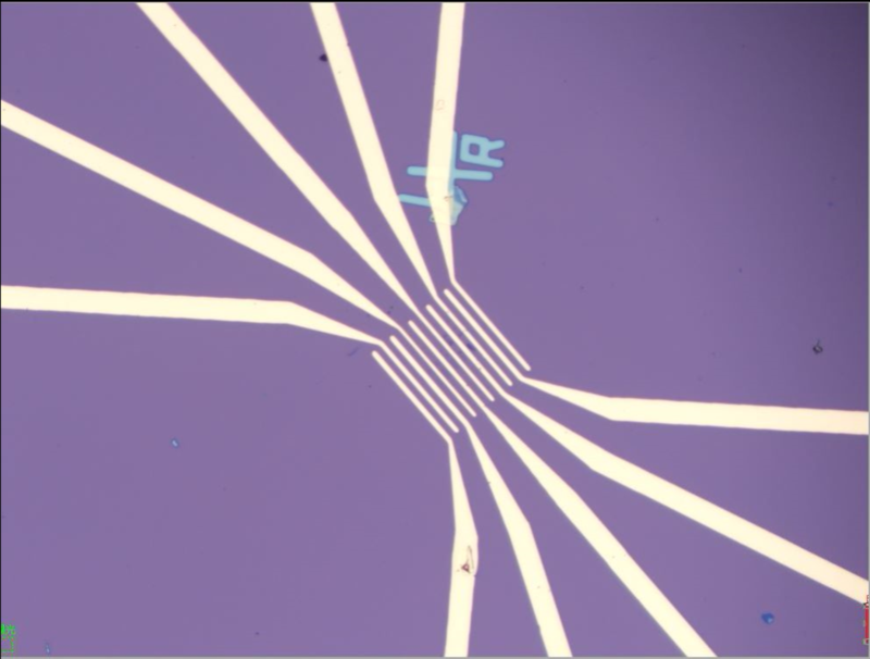
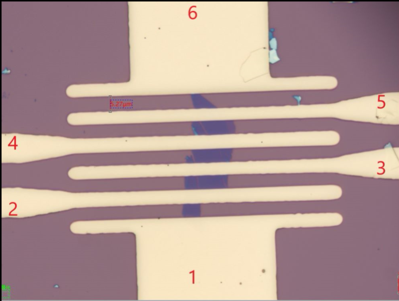
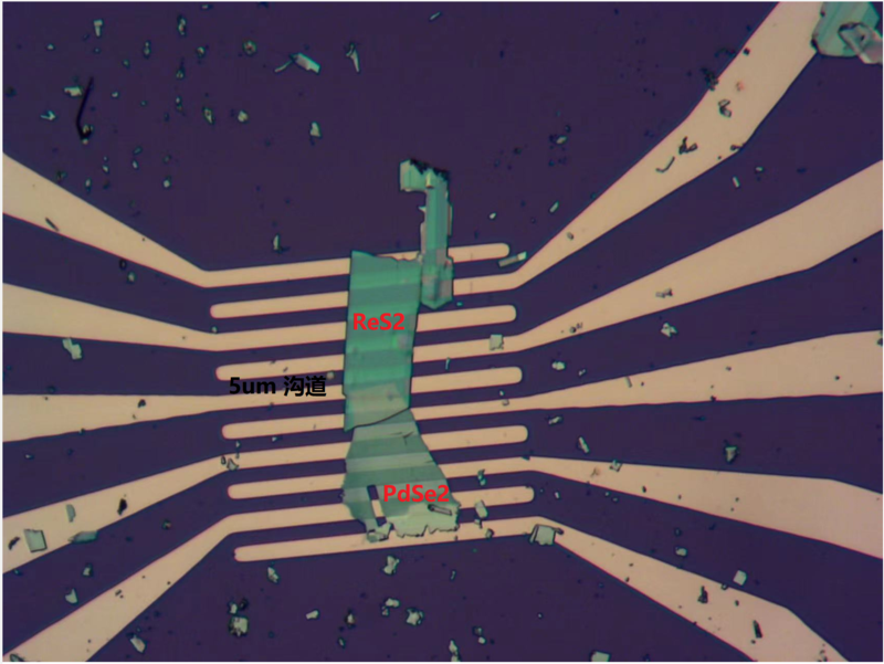
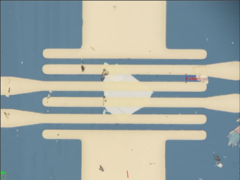
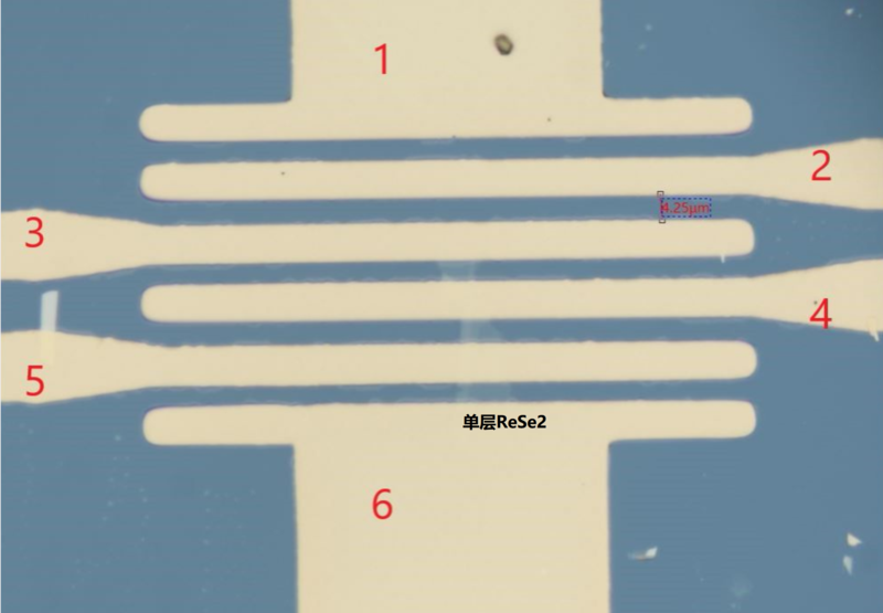
TSV technology (through-silicon through-hole technology), generally referred to as through-silicon through-hole technology, is a new technical solution for interconnecting stacked chips in three-dimensional integrated circuits. TSV can make the density of the chips stacked in the three-dimensional direction the largest, the shortest interconnection between the chips, the smallest size, and greatly improve the performance of chip speed and low power consumption. Beike Nano masters the latest TSV technology, which can help customers to complete TSV personalized requirements.

Technology application

As one of the most promising technologies in microelectronics manufacturing, TSV technology has been widely used in MEMS devices, memory, image sensors, power amplifiers, biological application equipment and various mobile phone chips.

Process capability

Through hole diameter: 20-30um Aspect ratio: 10: 1 Through-hole materials: copper, gold Through hole status: solid hole, hollow hole

Our advantage

Graphics can be customized High through hole yield Can be mass produced Process technology is mature


Warm tip: the products supplied by Beijing Beike Xincai Technology Co., Ltd. are only used for scientific research, not for human body

Message
Full name: *
Whatsapp/Wechat: *
E-mail: *
Contents:
 
Twitter:2D materials Frontier
QQ Exchange Group:1092348845


Reminder: Beijing Beike New Material Technology Co., Ltd. supplies products only for scientific research, not for humans
All rights reserved © 2019 beijing beike new material Technology Co., Ltd 京ICP备16054715-2号
advisory
phone
Email:mxenes@163.com
Tel:+86-17715390137
scan

scan
WeChat