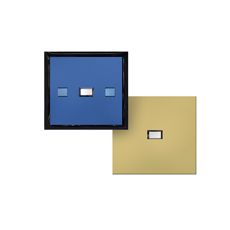
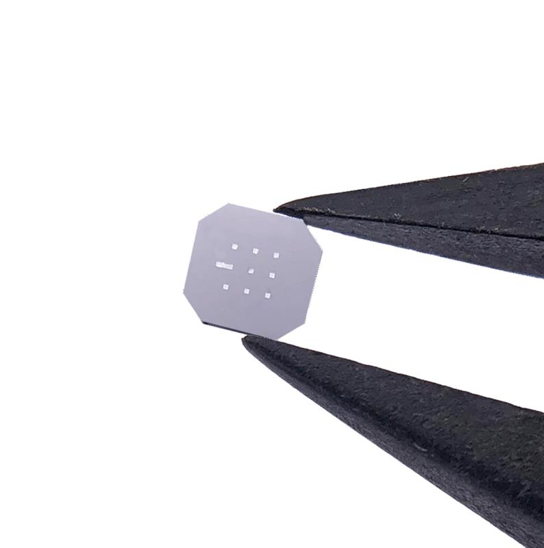
TL-400 liquid chip can realize high-resolution in-situ TEM liquid observation, and the resolution can reach more than 1nm. There is a 40 x 40 x 0.1um silicon nitride film observation window in the middle of the liquid chip. There are a liquid drip port and a negative pressure liquid suction port on the left and right sides of the chip.
In the in-situ experiment, the liquid to be tested is first dropped into the liquid dropping port, and the matched negative pressure device is used to suck the liquid to be tested into the liquid chamber through the negative pressure, and then the two liquid dropping windows are sealed with epoxy resin. In-situ liquid observation can be performed after the glue is cured. TL-400 can be applied to the following research and analysis:
Observation and analysis of liquid environmental samples of equipment such as TEM, SEM and Raman;
In situ chemical reaction observation, crystal growth and corrosion in situ study;
Observe and study biological samples such as live bacteria and cells in the liquid environment.
―― TL-400 in-situ TEM liquid chip ――
|
Product ID
|
Film thickness
|
Liquid chamber size
|
Observation window size
|
Frame size
|
|
|
TL-400
|
30nm
|
40 x 40 x 0.1 um
|
40 x 40 um
|
3mm
|
|
|
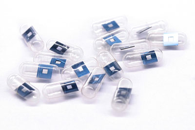
Each box contains 10 chips
|
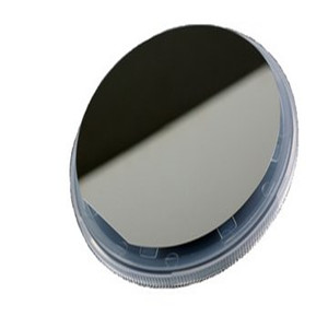
Case show
Synchrotron radiation / SEM in-situ liquid chip
The TBL-500 liquid chip can realize high-resolution in-situ synchrotron radiation and SEM liquid (compatible with scanning transmission mode) observation. There is a large vacuum-resistant silicon nitride film observation window of 400 x 800 x 1um in the middle of the liquid chip. There are a liquid drip port and a negative pressure liquid suction port on the left and right sides of the chip.
In the in-situ experiment, the liquid to be tested is first dropped into the liquid dropping port, and the matched negative pressure device is used to suck the liquid to be tested into the liquid chamber through the negative pressure, and then the two liquid dropping windows are sealed with epoxy resin. In-situ liquid observation can be performed after the glue is cured. TBL-500 can be used for:
Observation and analysis of liquid environment samples of equipment such as synchrotron radiation, SEM and Raman; In situ chemical reaction observation, crystal growth and corrosion in situ study; Observe and study biological samples such as live bacteria and cells in the liquid environment.
―― TBL-500 in-situ SEM liquid chip ――
|
Product ID
|
Film thickness
|
Liquid chamber size
|
Observation window size
|
Frame size
|
|
|
TBL-500
|
100nm
|
400 x 800 x 1 um
|
400 x 800 um
|
6 x 6 mm
|
|
|
Each box contains 10 chips
|
Case show

TEM observation of in situ reaction of Ag and S (TL-400)
|
Warm tip: the products supplied by Beijing Beike Xincai Technology Co., Ltd. are only used for scientific research, not for human body |
| Item ID |
CAS |
ID |
Pack |
Parameter |
Stock |
Make up |
Price |
| BK2020050501-01 |
51-18-3 |
BK2020050501 |
TL-400 |
|
100 |
|
$1560 |
| BK2020050501-02 |
51-18-3 |
BK2020050501 |
TBL-500 |
|
100 |
|
$1380 |