registered   |   log in
  中文

北科产品中心 products center

MXenes-Max 2D transition metal carbonitride
MBene two-MAB-dimensional transition metal borides
MOFs metal organic framework compound
COFs covalent organic compound
Bioluminescent dyes
Aerogels
CVD TMDC 2D thin film / heterojunction
Perovskite material
Copper-doped modified lead apatite (LK 99 crystal powder)
2D material fiber/film
Two-dimensional material micro-nano processing - in situ testing
Basic magnetic beads, immunomagnetic beads, protein purification magnetic beads, nucleic acid extraction magnetic beads
Nucleic acid extraction kit
High-entropy materials
Biological nanomaterials
Nanocellulose
AIE luminescent material
Silane Bismuthene Borene Tellurene Phosphorene Graphyne
Binary CVD TMDC crystal/powder/dispersion
Ternary CVD TMDC crystal/powder/dispersion
Graphene and carbon nanomaterials
High-performance battery materials
Carbon nanotube/fullerene series
Nano/micron powder material and AAO template
Nanowires
Molecular sieve
Ionic liquid
QDS
Nanomaterial customization / material simulation calculation
Metal nanomaterials
Hydrogel Series and Consumables
Solid-state lithium battery
Product Solutions
Industrial-grade nanomaterials
Special materials for sodium storage
Thermoelectric materials
Organic materials
Atomic catalyst
Mesoporous materials
Heavy launch-new products are online!
Two-dimensional layered double hydroxide
catalyst
Nanosphere
Material testing and consumables
Inorganic Nanomaterials
equipment
MXenes 2D transition metal carbonitride
MBene two-dimensional transition metal borides
beike new material
position: home > Product > Material testing and consumables

SEM scanning electron microanalysis


ID:BK2020011706
CAS:
price: Inquiry
Item ID:BK2020011706-04
specification:
Detailed

Detailed consultation with customer service


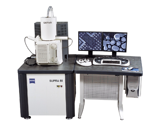
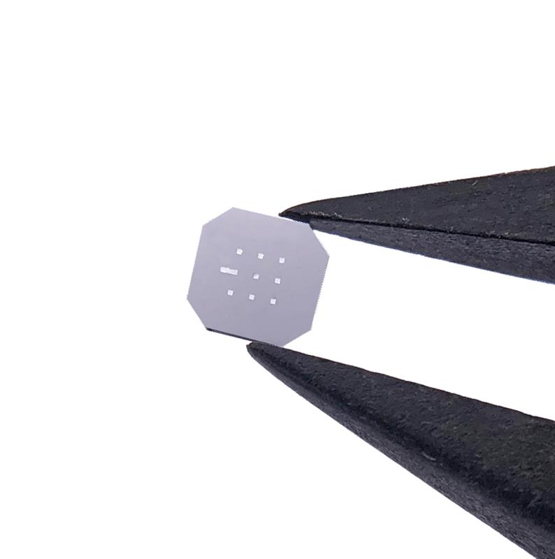
Surface morphology observation


Electron microanalysis is to analyze the micro region morphology, crystal structure and chemical composition of the sample material by using various physical signals generated by the interaction between the focused electron beam and the sample material.

The manufacture of SEM is based on the interaction between electron and matter. When a high-energy incident electron bombards the surface of the material, the excited region will produce secondary electron, Auger electron, characteristic X-ray and continuous spectrum X-ray, backscatter electron, transmission electron, and electromagnetic radiation in the visible, ultraviolet and infrared light regions. At the same time, it can also produce electron hole pair, lattice vibration (phonon), electron vibration (plasma). In principle, by using the interaction of electrons and matter, we can obtain the information of various physical and chemical properties of the sample itself, such as morphology, composition, crystal structure, electronic structure, internal electric field or magnetic field, etc.

According to the mechanism of different information, different information detectors are used to realize the selective detection. For example, collecting the secondary electron and backscattered electron can get the information about the micro morphology of the substance, and collecting the X-ray can get the information about the chemical composition of the substance.


Warm tip: the products supplied by Beijing Beike Xincai Technology Co., Ltd. are only used for scientific research, not for human body

Item ID CAS ID Pack Parameter Stock Make up Price
BK2020011706-01 BK2020011706 表面形貌观察 100 $0
BK2020011706-02 BK2020011706 微区元素分析 100 $0
BK2020011706-03 BK2020011706 断口形貌分析 100 $0
BK2020011706-04 BK2020011706 EBSD 100 $0
Message
Full name: *
Whatsapp/Wechat: *
E-mail: *
Contents:
 
Twitter:2D materials Frontier
QQ Exchange Group:1092348845


Reminder: Beijing Beike New Material Technology Co., Ltd. supplies products only for scientific research, not for humans
All rights reserved © 2019 beijing beike new material Technology Co., Ltd 京ICP备16054715-2号
advisory
phone
Email:mxenes@163.com
Tel:+86-17715390137
scan

scan
WeChat