

 Application
New Nature: Wafer-level single crystal hexagonal boron nitride single layer
QQ Academic Group: 1092348845
Detailed
【introduction】
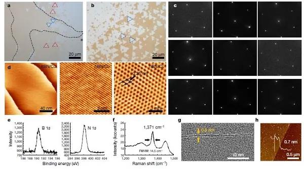
Ultra-thin two-dimensional semiconductor layered materials are believed to effectively extend Moore‘s Law of integrated circuit transistors. The key challenge currently facing 2D semiconductors is how to avoid the formation of charge scattering and trap sites in adjacent dielectrics. More and more studies have shown that the insulating van der Waals layer of hexagonal boron nitride (hBN) can provide excellent interfacial dielectric properties while effectively reducing charge scattering. However, how to achieve reliable single crystal hexagonal boron nitride thin film growth on wafers has become a technical difficulty that must be tackled in the industry.
[Achievement Profile]
[Picture and text guide]
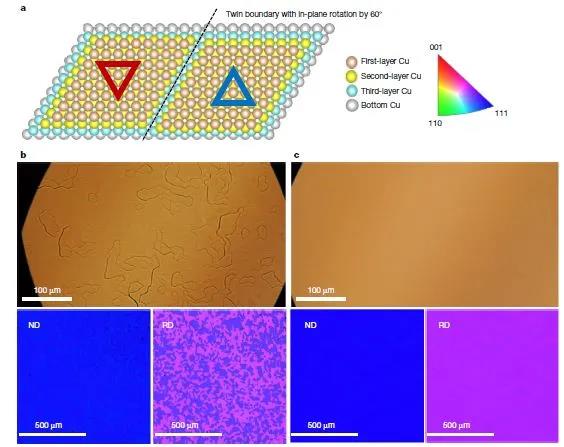


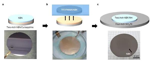
Literature link: Wafer-scale single-crystal hexagonal boron nitride monolayers on Cu (111) (Nature, 2020, DOI: 10.1038 / s41586-020-2009-2)
- Previous: [Nano] Angew. Chem .:
- Next: Engineering bacteria p