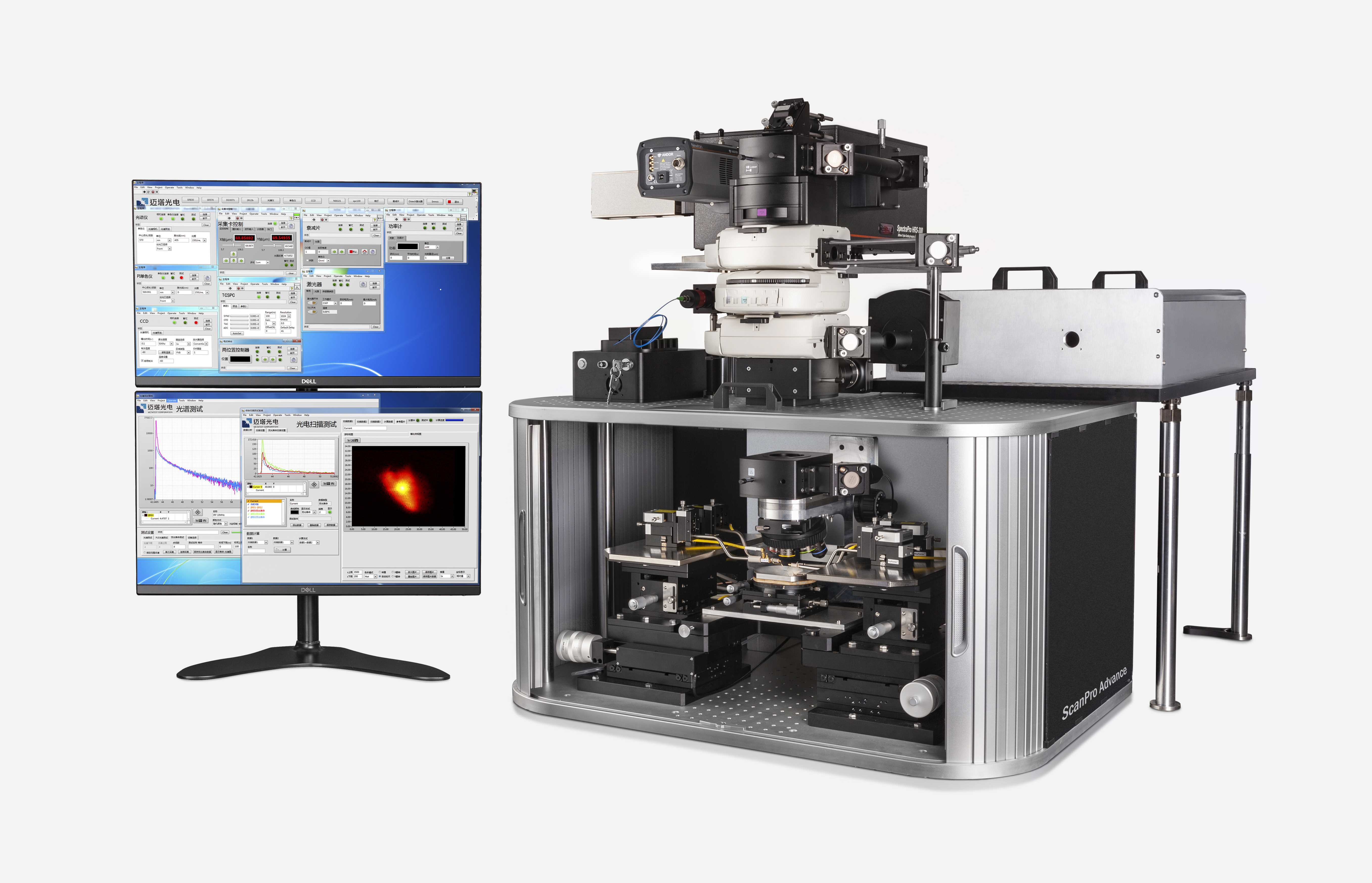
ScanPro Advance is a highly-functional and customized multi-functional photoelectric test system. The flexible configuration can meet complex customized requirements. Raman spectroscopy, fluorescence spectroscopy, steady state / transient photocurrent testing, absorption spectroscopy, fluorescence lifetime testing, electroluminescence testing can be integrated on a single device, and spectral scanning and photocurrent can be performed with a high-precision pressure level shifter Scanning and fluorescence lifetime scanning. The ultra-high stability microscope structure can support continuous testing for a long time. The multilayer optical light path can be tested using a variety of light sources including continuous output lasers, picosecond pulse lasers, halogen lamps, xenon lamps and so on.
The main technical parameters*
gain
4x, 10x, 20x, 50x ultra-long working distance objective lens, working distance greater than 18mm
100x semi-apochromatic objectives
Optional 15x, 40x achromatic objectives, 480-1800nm long working distance infrared objectives
Excitation light source
405nm, 520nm, 635nm semiconductor laser, 532nm solid state laser
Optional 450nm, 488nm, 505nm, 650nm semiconductor laser
405nm, 445nm picosecond laser
Continuously adjustable xenon lamp / supercontinuous laser light source
Excitation light path module 405nm laser fluorescence spectrum test module, 532nm laser Raman spectrum test module, photocurrent test homogenization illumination light path module, photocurrent test focus spot illumination module
Spectrometer configuration 328mm focal length 4 grating spectrometer, deep-cooled front-illuminated CCD, refrigeration temperature -60 degrees
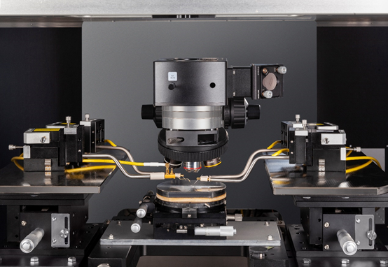
Probe station is equipped with 4 probe fixtures, with 5 micron tip probes, triaxial connection, leakage current is less than 1pA
Raman spectrum test range: 180-4000 wavenumbers (optional 90-4000 wavenumbers and 35-4000 wavenumbers)
Fluorescence spectrum test range 430-1000nm (405nm excitation), 540-1000nm (532nm excitation)
Scanning range: 100um each in XY direction
Scanning point spacing minimum 50nm
Spatial resolution 400nm (Raman / fluorescence spectral scanning), 1μm (photocurrent scanning)
Optional modules Absorption spectrum test module, polarization spectrum test module, electroluminescence spectrum test module, fluorescence emission spectrum (PLE) test module, fluorescence life test module, electroluminescence (EL) spectrum test module, xenon lamp module, UV / IR No chromatic aberration optical path module.
ScanPro Advance structural design
High stability optical light path
ScanPro Advance uses a high-stability microscope stand design for long-term stable testing.


ScanProAdvance uses a high-stability microscope stand design, which is suitable for long-term stable testing. Using a 100x objective lens to observe the sample, there was no visible change for more than 3 hours.
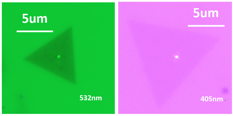
Multi-color illumination assisted focusing
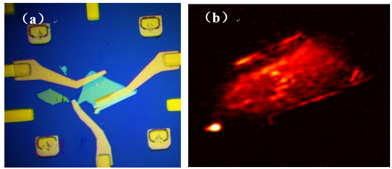
Five color filters can change the color of the illumination light. By using colored light with a wavelength close to the laser light and adjusting the focus, you can ensure that the laser spot is accurately focused on the sample surface.
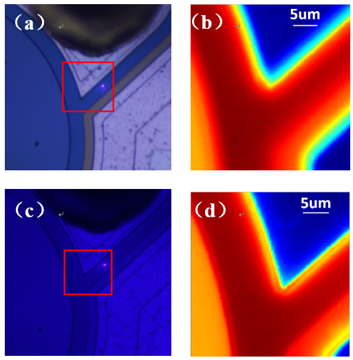
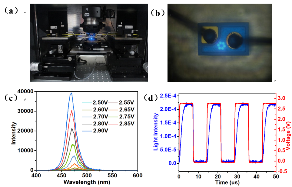
If you use a white illumination light source and adjust the 405nm laser to the smallest spot size, because the imaging optical path has chromatic aberration, the actual laser is not focused on the sample surface, and the photocurrent scanning effect is poor, as shown in Figure b. However, if the purple illuminating light source is used to adjust the 405nm laser focus, the chromatic aberration of the imaging system can be compensated because the illuminating light source and the laser wavelength are similar, so that the laser light can be accurately focused on the sample surface and a high-resolution photocurrent scanning image can be obtained, as shown in Figure d.
Stacked light path
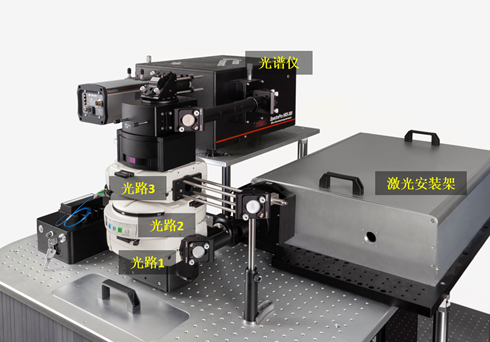
ScanPro Advance can use up to 3 layers of incident light path, and each layer of incident light path can be installed with up to 5 beam splitters or dichroic mirrors. You can also use a laser mounting bracket to mount up to 3 free-space output lasers in a hood. Therefore ScanPro Advance provides a very rich optical extensibility, which can support complex optical tests.
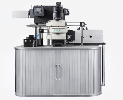
Enclosed enclosure design completely shields from ambient light.
Photocurrent test function

Light spot type (a) Homogenized lighting spot, (b) Laser lighting spot
ScanPro Advance offers two different types of illumination spots in the photocurrent test. The homogenization lighting module converts the laser light into a uniform small light spot and irradiates the sample, and provides a white LED as an indicator light to indicate the laser irradiation position. The spot size is at least 8 microns (50x objective). The uniform light spot also facilitates the calculation of the optical power density during the test. The focused illumination spot focuses the laser light directly on the sample surface to form a tiny Gaussian spot with a spot size of about 1 micron. It can be positioned at a specified position to excite the sample and also used for photocurrent scanning.
Photocurrent scanning test (a) bright field, (b) corresponding area scan
Using a high-precision piezoelectric stage, ScanPro Advance can perform scanning with a positioning accuracy of up to 20nm in the range of up to 100 microns. Since the spot size is about 1 μm, the spatial resolution of the photocurrent scanning is also 1 μm. During the photocurrent scanning, the dark current will also change with time due to changes in the device itself or air interference. If the light response of the device is weak, the change in dark current during scanning may be the same as that of photocurrent, making the image unusable. Metatest Suite measures the photocurrent and dark current at each data point by controlling the laser switch. Because the time interval between two tests at each data point is short and the dark current changes are small, the photocurrent value of the device can be accurately measured to obtain a high-resolution photocurrent scan image. The optional lock-in amplifier for photocurrent scanning can also avoid the effects of dark current fluctuations.
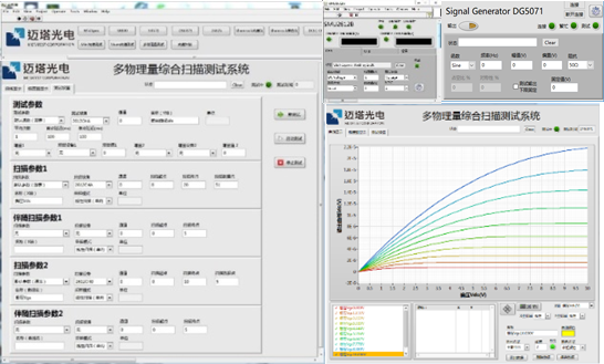
Package example
The Metatest Suite software package controls the test equipment in all systems in a unified manner, and can scan the parameters of up to 4 (2 groups) parameters with all efforts, so that it can measure the photocurrent curves under different light intensity and voltage at one time.
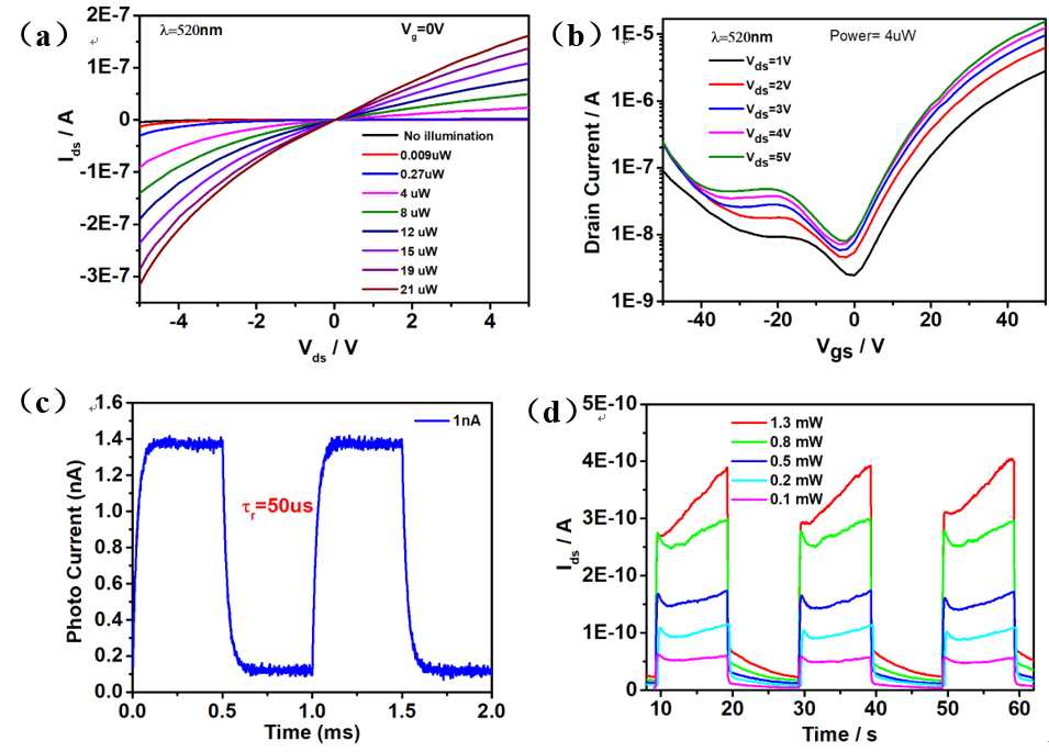
Test example (a) Output curve of variable intensity measurement, (b) Transfer curve of fixed intensity measurement
(C) Light response test, (d) Variable light intensity test switch ratio
Spectrum test function
The 405nm fluorescence spectrum test optical path and the 532nm Raman spectrum measurement optical path have been specifically optimized for two wavelengths of laser light. When using a 100x objective lens, it has a diffraction-limited spot, so it can provide extremely high spatial resolution in spectral scanning.
ScanPro Advance uses a free-space optical path design. The Raman / fluorescence signal of the sample is directly focused on the spectrometer slit through the mirror, which has a high collection efficiency. The spectrometer uses a cold-type detector with extremely low thermal noise for long-term integration, which combines to ensure the accuracy of weak spectral testing. Utilizing a high-precision piezoelectric stage, ScanPro Advance can perform scanning with a positioning accuracy of up to 20nm in the range of up to 100 microns. Because the spot size is around 500nm (532nm laser), the spatial resolution of the spectral scan is also 500nm. Scanpro Advance spectral testing software has fast processing of spectral Mapping data, automatic smoothing, automatic calculation of integration, average, peak position, peak width and other information.
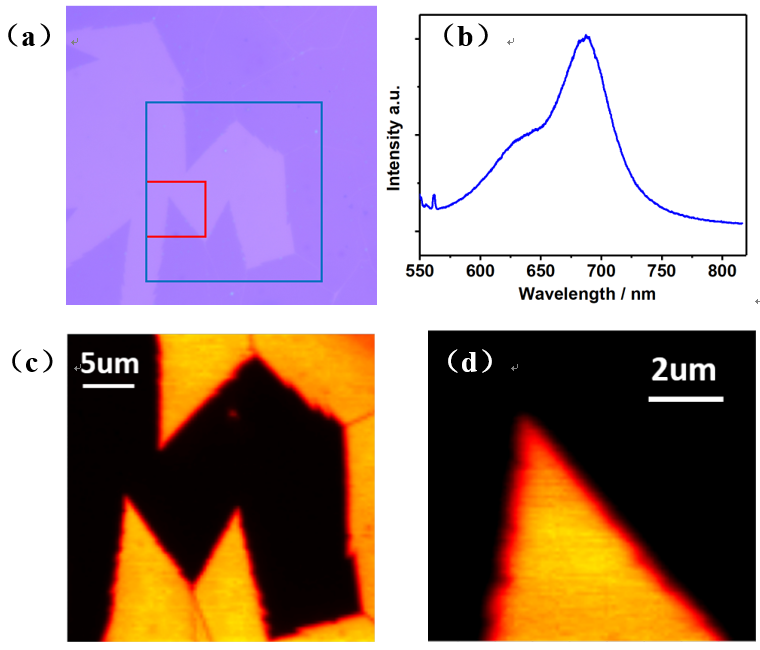
Example of fluorescence spectrum and scanning test (a) Bright field diagram of SiO2 / Si substrate MoS2 under 100X objective lens, blue frame is large area, red frame is small area (b) PL spectrum, (c) scanning area 30 * 30um, (d ) Scanning area 10 * 10um
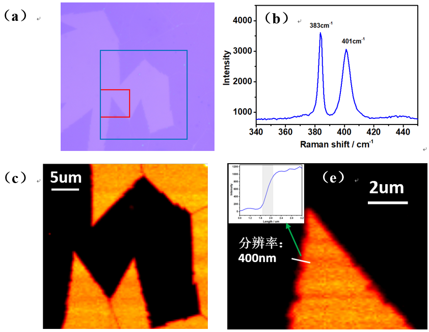
Example of Raman spectroscopy and scanning test (a) Bright field diagram of SiO2 / Si substrate MoS2 under 100X objective lens, blue frame is large area, red frame is small area (b) Raman spectrum, (c) scanning area 30 * 30um, d) Scanning area is 13 * 10um, the illustration is a Raman scan cut-line diagram, showing the scanning resolution is 400nm
Polarization spectrum test
ScanPro Advance is equipped with an electric polarizer and an electric analyzer, which can automatically adjust the polarization direction of the incident laser light. The polarizer uses a fixed polarizer and a rotatable half-wave plate, and the laser energy does not change during the process of changing the polarization direction. The analyzer uses a broadband polarizer, which can cover the wavelength range of 250-4000nm. Metatest Suite test software can automatically rotate the polarizer or analyzer, or synchronously rotate the polarizer and analyzer. During the rotation process, the spectral data can be automatically recorded to quickly measure the polarization spectrum data of the sample.
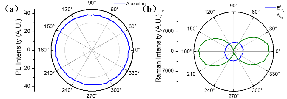
Example of Polarized Fluorescence and Raman Testing Using (532) Laser Excitation to SiO2 / Si Substrate MoS2 by (a) Polarized Fluorescence Spectrum and (b) Polarized Raman Spectroscopy Test
Fluorescence lifetime spectroscopy and mapping
Scapro Advance can be optionally equipped with a fluorescence lifetime test function. The instrument channel width is 64ps, which is suitable for samples with fluorescence lifetimes over 500ps, such as perovskite and quantum dots. The detector is mounted on the spectrometer and can scan the spectrum by rotating the grating to obtain a life curve of the sample at different wavelengths. For short-life samples, a tcspc test system with a minimum time channel width of 813fs can be selected. With a high-speed detector and picosecond laser, the instrument has a response speed of about 22ps and can measure fluorescence lifetimes greater than 10ps.
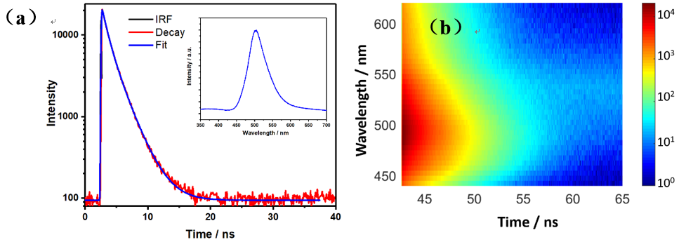
Fluorescence lifetime test (a) Fluorescence lifetime spectrum of green crystal, inset is PL spectrum,
(B) Fluorescence lifetime graphs at different wavelengths
With the high-resolution sample scanning test system, fluorescence lifetime mapping can also be performed. The data processing software can automatically process the mapping data, fit with up to 3 indices, and directly generate a Mapping image with different parameters.
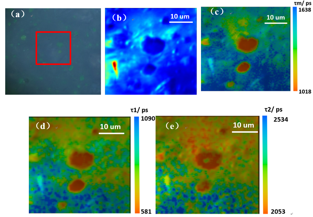
Fluorescence lifetime scan test (a) Brightfield picture, (b) Fluorescence lifetime scan intensity diagram, (c) Fluorescence lifetime scan fit average lifetime diagram, (d) Fluorescence lifetime scan fit τ1 lifetime diagram, (c) Fluorescence lifetime scan Fitting τ2 life graph
Absorption spectroscopy
ScanPro Advance can be equipped with halogen light source for absorption spectrum test, with a spectral range of 390-1100nm.

Indicating fiber diagram under 50X objective lens
With the indicator fiber, the position of the spectrum collection can be directly observed to measure the spectrum of the specified area. ScanPro Advance uses a 100-micron fiber to collect the reflected light from the sample. The measurement area is only 2 microns under a 100x objective lens, so that it can easily measure the absorption spectrum of a specified area of a small sample.
With the advantages of high sensitivity and low noise of the back-illuminated miniature spectrometer, the single spectral test time is only 5ms, and the absorption spectrum of the sample can be accurately measured on multiple spectra.
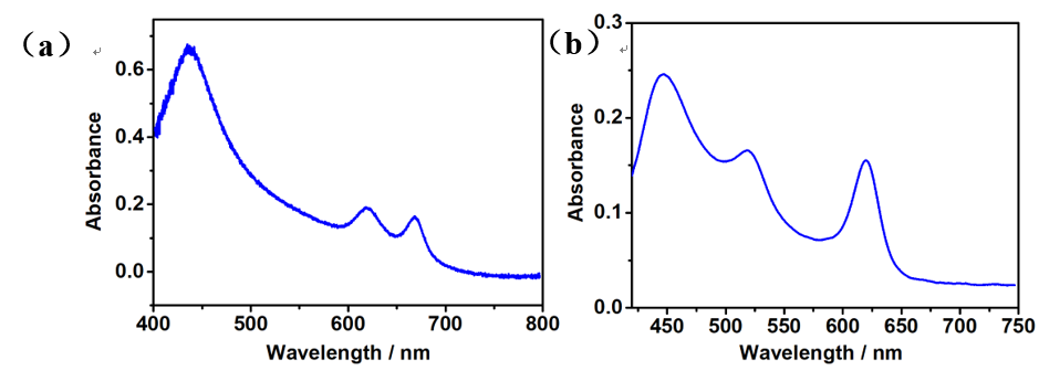
(A) Sapphire substrate MoS2 (b) Sapphire substrate WS2
Electroluminescence spectrum test function
The electroluminescence spectrum module can measure the electroluminescence spectrum of the sample. The refrigerated back-illuminated CCD spectrometer has sensitive light response and can measure the weak luminescence of the sample. The measurement range is 300-1100nm. In the Metatest Suite software package, the excitation voltage of the sample can be scanned automatically and the emission spectrum can be measured. The photodetector can be used to measure the response speed of the sample‘s luminescence on the microsecond scale. Depending on the sensitivity of the sample, a silicon detector or a PMT detector can be selected to measure the light intensity emitted by the sample.
Electroluminescence test
(C) Electroluminescence spectra of samples under different bias voltages, (d) Transient characteristics of electroluminescence
Continuously variable wavelength light source
Fluorescence emission spectrum (PLE) test function

The mXenon xenon lamp module uses a colorless optical system, which ensures consistent spectral resolution from ultraviolet to infrared and higher ultraviolet light intensity. The optical power density in the 240-700nm band is greater than 20mW / cm2 (spot size 13.3μm). Optically optimized shutters and choppers provide high-speed switching speeds (shutter opening / closing time 900 μs, chopper opening / closing time 20 μs at 1 kHz).
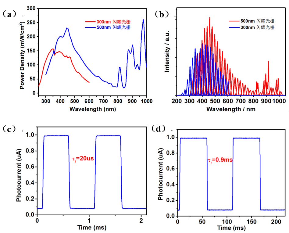
(A) Optical power density at different wavelengths of 300nm and 500nm blazed gratings, (b) Spectra at different wavelengths of 300nm and 500nm blazed gratings, (c) Chopper switching speed, (d) Shutter switching speed
In addition to adjusting the output light intensity through software, the electric attenuator wheel also has a constant power output mode, which automatically adjusts the light intensity according to the output light wavelength to generate a fixed-power lighting source. Using a constant-power light source, you can measure the response rate of a sample at a specified light intensity and the I-V curve of the sample under different wavelength excitations.
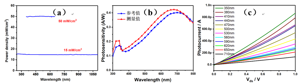
a) Constant power output mode, at a wavelength of 250-1100nm, fixed lighting optical power density 15mW / cm2, output power stability 3%, output curve and at a wavelength of 350-650nm, fixed lighting optical power density 50mW / cm2, power 1% stability. Illumination range is 13 microns in diameter. (B) The silicon detector response rate curve (red line) measured at a fixed illumination optical power density of 15 mW / cm2. The blue line is the reference value. (C) I-V curves at different wavelengths.
By changing the wavelength of the excitation light to excite the fluorescence of the sample, and fixing the excitation light power, the spectrometer can measure the fluorescence emission spectrum (PLE) of the sample. The Metatest Suite can automatically change the wavelength of incident light and record the fluorescence spectrum to quickly obtain PLE data.
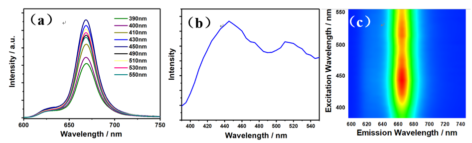
(A) PLE spectrum diagram of SiO2 / Si substrate MoS2, (b) integral spectrum of emission spectrum in the wavelength range of 650-700nm at different excitation wavelengths, and (c) two-dimensional intensity diagram of emission spectrum at different excitation wavelengths.
source:https://www.metatest.cn
|
Warm tip: the products supplied by Beijing Beike Xincai Technology Co., Ltd. are only used for scientific research, not for human body |